The preparation and characterization of copper aluminum diselenide (CuAlSe2) and Titanium dioxide (TiO2)-doped with carbon based graphene nanocomposite thin films were examined. The temperature, deposition time, and pH of the medium was varied by spin coating method. Samples were characterized by X-ray diffraction (XRD), field emission scanning electron microscopy (FESEM) and energy dispersive x-ray (EDX) and UV visible spectroscopy techniques for the structural, morphological, compositional features and photo-response for photovoltaic devices. The optical property revealed that CuAlSe2 films have energy band gaps range 2.22-5.80 eV and 2.10-2.14 eV at room and peak temperature. The XRD patterns of CuAlSe thin films showed peaks (101), (102), (006), (110), (108), and (116) corresponding to the formation of hexagonal phase of CuInSe2 and the particle size D 38.20 nm. XRD pattern of C: CuAlSe2 and TiO2 flakes were perfectly crystallized and the inter-planar spacing of 0.053 nm. FESEM analysis indicated smooth and uniform structures. The graphene-TiO2 displayed glistering surfaces due to less density of electronic trap states and improved absorption in the UV region. The resistivity of the samples were 1.95s/m and 12.93s/m for GO and GO-TiO2. The results indicated that the average electron mobility depends on the probability of the electrons in the conduction band and as the quasi-Fermi level approaches the CB, a higher current, power supply and lower resistivity level.
| Published in | Journal of Photonic Materials and Technology (Volume 11, Issue 1) |
| DOI | 10.11648/j.jpmt.20261101.12 |
| Page(s) | 7-15 |
| Creative Commons |
This is an Open Access article, distributed under the terms of the Creative Commons Attribution 4.0 International License (http://creativecommons.org/licenses/by/4.0/), which permits unrestricted use, distribution and reproduction in any medium or format, provided the original work is properly cited. |
| Copyright |
Copyright © The Author(s), 2026. Published by Science Publishing Group |
Graphite, Graphene, CuAlSe2 C, TiO2-GO, CuSe, Spin Coating
Graphene | Thickness t () | V (mv) | I (A) | () | m) | m | References |
|---|---|---|---|---|---|---|---|
TiO2 | 0.022 | 28.0 | 5.47 | 23.20 | 0.5104 | 1.93 | This study |
RGO- CuAlSe2 | 0.015 | 50.0 | 44.01 | 5.15 | 0.0773 | 12.94 | This study |
RGO-TiO2 | 0.022 | 14.6 | 3.70 | 17.88 | 0.3934 | 2.54 | This study |
CuAlSe2 | 0.015 | 53.0 | 90.65 | 2.65 | 0.0398 | 25.13 | This study |
GO-NGF | 0.027 | 25.0 | 4.95 | 22.90 | 0.6183 | 1.62 | |
RGO-NGF | 50.0 | 45.69 | 4.95 | 0.1330 | 7.52 | ||
RGO | 0.025 | - | - | 0.0179 | - | 23.30 | |
CuSe | - | - | - | - | 10.0 | 0.001 | |
CuInSe2 | - | 300.0 | - | - | 1.03 | 0.97 |
CuAlSe2 | Copper Aluminum Diselenide |
TiO2 | Titanium Dioxide |
XRD | X-ray Diffraction |
FESEM | Field Emission Scanning Electron Microscopy |
EDX | Energy Dispersive x-ray |
SMOs | Semiconducting Metallic Oxides |
PSCs | Perovskite solar cells |
Al2(SO4)3.14H2O | Aluminum Trisulphate |
CuCl2.2H2O | Copper Chloride |
Na2SeSO4 | Sodium Selenosulphate |
[Na2EDTA] (C10H14N2Na2O8.H2O) | Disodium Ethylene Diaminetetraacetic Acid |
RGO | Reduced Graphene Oxide |
FTO | Fluorine-doped tin Oxide |
SEM | Scanning Electron Microscopy |
FWHM | Full Width at Half Maximum |
nCB | Density of Electrons |
EFn | Quasi-Fermi Level |
| Boltzmann’s Constant |
Sample A | GO |
Sample B | RGO |
Sample C | CuAlSe2-GO |
Sample D | TiO2-GO |
CB | Conduction Band |
| [1] | Geim, A. K., Novoselov, K. S. The Rise of Graphene. Nature Materials, 2007 6 183-191 |
| [2] | Paulchamy B, Arthi G, Lignesh BD A Simple Approach to Stepwise Synthesis of Graphene Oxide Nanomaterial. J Nanomed Nanotechnology 2015 6: 253. |
| [3] | Roose, B., Sandeep P., & Ullrich S., Doping of TiO2 for sensitized solar cells (Review), 2015 Chem. Soc. Rev., 44, 8326-8349 |
| [4] | Coros, Maria; Pogacean, Florina; Turza, Alexandru; Dan, Monica; Berghian-Grosan, Camelia; Pana, Ioan-Ovidiu; Pruneanu, Stela. Green synthesis, characterization and potential application of reduced graphene oxide. Physica E: Low-dimensional Systems and Nanostructures, 2020, 113971 |
| [5] | Ladan H. A and Buba A. D. A Synthesis, Characterization and Simulation of 2D Graphene for Perovskite Solar Cells, Ph.D Thesis, Department of Physics, Faculty of Science, University of Abuja, Nigeria, 2021 phyfosuofA-21/15538006/07/2021 |
| [6] | Sengupta, D., P. DAS, Mondal B., & Mukherjee K., Effect of doping, morphology and film-thickness of photo-anode materials for Dye sensitized solar cell application- A review Renewable Energy Reviews 206, 60, 356-376 |
| [7] | Eluyemi, M. S., Eleruja, M. A., Adedeji, A. V., Olofinjana, B., Fasakin, O., Akinwunmi, O. O.,... & Ajayi, E. O. B. Synthesis and characterization of graphene oxide and reduced graphene oxide thin films deposited by spray pyrolysis method. Graphene, 2016, 5(3), 143-154. |
| [8] | Campillo C., Fortes R., & Prieto M. H. Solar Radiation Effect on Crop Production, Centro de Investigaciónn finca la Orden-Valdesequera, Spain. 2019. |
| [9] | Landmann M., E Rauls and W G Schmidt The electronic structure and optical response of rutile, anatase and brookite TiO2, J. Phys.: Condens. Matter, 2012, 24, 195503 6pp |
| [10] | Zaabaa N. I Hummers Method: Solvent Influence, Procedia Engineering, 207, 184 469-477. |
| [11] | Hu, W., Yang, S., and Yang, S. Surface Modification of TiO2 for Perovskite Solar Cells. Trends in Chemistry, 2019. |
| [12] | Kumar, M., Raj, A., Kumar, A., and Anshul, A. An optimized lead-free formamidinium Sn-based perovskite solar cell design for high power conversion efficiency by SCAPS simulation. Optical Materials, 2020, 108, 110213. |
| [13] | Gagandeep, Singh, M., Kumar, R., & Singh, V. Investigating the impact of layer properties on the performance of p-graphene/CH3NH3PbI3/n-csi solar cell using numerical modelling. Superlattices and Microstructures, 2020, 106468. |
| [14] | Ladan A. H; and Bello A., Extraction and Characterization of Okaba Natural Coal obtained from Kogi state Nigeria, Undergraduate Project, Department of Physics, Saadu Zungur University, Bauchi State, Nigeria, 2024. |
| [15] | Wan X., Long, G., and Chen, Y. Graphene for Transparent Electrodes and Organic Electronic Devices. Green Energy and Technology, 2012, 81-102. |
| [16] | Gurin, Valerij and Alexeenko, A. A., X-ray Diffraction and Electron Microscopy Study of the Novel Plasmonic Optical Materials With Copper Selenide Nanoparticles, 2023. |
| [17] | Thirumavalavan, S., Mani, K., Sagadevan, S. ”Investigation of the Structural, Optical and Electrical Properties of Copper Selenide Thin Films”. Materials Research, 2015, 18(5), 1000-1007. |
| [18] | Oikkonen LE, Ganchenkova MG, Seitsonen P and Nieminen RM. Redirecting focus in CuInSe2 research towards selenium-related defects. Physical Review B: Condensed Matter and Materials Physics. 2012; 86(16): 165115. |
| [19] | Hankare, P. P., Khomane, A. S., Chate, P. A., Rathod, K. C., and Garadkar, K. M. Preparation of copper selenide thin films by simple chemical route at low temperature and their characterization. Journal of Alloys and Compounds, 2008, 469 (1-2), 478-482. |
| [20] | Garg, J. C., Sharma, R. P., Sharma, K. C. Characterization of p-CuInSe2 films for photovoltaic grown by a chemical deposition technique. Thin Solid Films, 1998, 164, 269-273. |
| [21] | Tell, B., & Wiegand, J. J. Photodetection properties of Cu2Se‐AgInSe2 heterojunctions. Journal of Applied Physics, 1977, 48(12), 5321-5323. |
| [22] | Paulson, P. D., Birkmire, R. W., & Shafarman, W. N. Optical characterization of CuIn1− x GaxSe2 alloy thin films by spectroscopic ellipsometry. Journal of Applied Physics, 2003, 94(2), 879-888. |
APA Style
Aminu, L. H., Buba, A. (2026). Optical and Structural Properties of TiO2 and CuAlSe2 Doped with Carbon Based Graphene for Photovoltaic Devices. Journal of Photonic Materials and Technology, 11(1), 7-15. https://doi.org/10.11648/j.jpmt.20261101.12
ACS Style
Aminu, L. H.; Buba, A. Optical and Structural Properties of TiO2 and CuAlSe2 Doped with Carbon Based Graphene for Photovoltaic Devices. J. Photonic Mater. Technol. 2026, 11(1), 7-15. doi: 10.11648/j.jpmt.20261101.12
AMA Style
Aminu LH, Buba A. Optical and Structural Properties of TiO2 and CuAlSe2 Doped with Carbon Based Graphene for Photovoltaic Devices. J Photonic Mater Technol. 2026;11(1):7-15. doi: 10.11648/j.jpmt.20261101.12
@article{10.11648/j.jpmt.20261101.12,
  author = {Ladan Haruna Aminu and Ada Buba},
  title = {Optical and Structural Properties of TiO2 and CuAlSe2 Doped with Carbon Based Graphene for Photovoltaic Devices},
  journal = {Journal of Photonic Materials and Technology},
  volume = {11},
  number = {1},
  pages = {7-15},
  doi = {10.11648/j.jpmt.20261101.12},
  url = {https://doi.org/10.11648/j.jpmt.20261101.12},
  eprint = {https://article.sciencepublishinggroup.com/pdf/10.11648.j.jpmt.20261101.12},
  abstract = {The preparation and characterization of copper aluminum diselenide (CuAlSe2) and Titanium dioxide (TiO2)-doped with carbon based graphene nanocomposite thin films were examined. The temperature, deposition time, and pH of the medium was varied by spin coating method. Samples were characterized by X-ray diffraction (XRD), field emission scanning electron microscopy (FESEM) and energy dispersive x-ray (EDX) and UV visible spectroscopy techniques for the structural, morphological, compositional features and photo-response for photovoltaic devices. The optical property revealed that CuAlSe2 films have energy band gaps range 2.22-5.80 eV and 2.10-2.14 eV at room and peak temperature. The XRD patterns of CuAlSe thin films showed peaks (101), (102), (006), (110), (108), and (116) corresponding to the formation of hexagonal phase of CuInSe2 and the particle size D  38.20 nm. XRD pattern of C: CuAlSe2 and TiO2 flakes were perfectly crystallized and the inter-planar spacing of 0.053 nm. FESEM analysis indicated smooth and uniform structures. The graphene-TiO2 displayed glistering surfaces due to less density of electronic trap states and improved absorption in the UV region. The resistivity of the samples were 1.95s/m and 12.93s/m for GO and GO-TiO2. The results indicated that the average electron mobility depends on the probability of the electrons in the conduction band and as the quasi-Fermi level approaches the CB, a higher current, power supply and lower resistivity level.},
 year = {2026}
}
TY  - JOUR
T1  - Optical and Structural Properties of TiO2 and CuAlSe2 Doped with Carbon Based Graphene for Photovoltaic Devices
AU  - Ladan Haruna Aminu
AU  - Ada Buba
Y1  - 2026/02/27
PY  - 2026
N1  - https://doi.org/10.11648/j.jpmt.20261101.12
DO  - 10.11648/j.jpmt.20261101.12
T2  - Journal of Photonic Materials and Technology
JF  - Journal of Photonic Materials and Technology
JO  - Journal of Photonic Materials and Technology
SP  - 7
EP  - 15
PB  - Science Publishing Group
SN  - 2469-8431
UR  - https://doi.org/10.11648/j.jpmt.20261101.12
AB  - The preparation and characterization of copper aluminum diselenide (CuAlSe2) and Titanium dioxide (TiO2)-doped with carbon based graphene nanocomposite thin films were examined. The temperature, deposition time, and pH of the medium was varied by spin coating method. Samples were characterized by X-ray diffraction (XRD), field emission scanning electron microscopy (FESEM) and energy dispersive x-ray (EDX) and UV visible spectroscopy techniques for the structural, morphological, compositional features and photo-response for photovoltaic devices. The optical property revealed that CuAlSe2 films have energy band gaps range 2.22-5.80 eV and 2.10-2.14 eV at room and peak temperature. The XRD patterns of CuAlSe thin films showed peaks (101), (102), (006), (110), (108), and (116) corresponding to the formation of hexagonal phase of CuInSe2 and the particle size D  38.20 nm. XRD pattern of C: CuAlSe2 and TiO2 flakes were perfectly crystallized and the inter-planar spacing of 0.053 nm. FESEM analysis indicated smooth and uniform structures. The graphene-TiO2 displayed glistering surfaces due to less density of electronic trap states and improved absorption in the UV region. The resistivity of the samples were 1.95s/m and 12.93s/m for GO and GO-TiO2. The results indicated that the average electron mobility depends on the probability of the electrons in the conduction band and as the quasi-Fermi level approaches the CB, a higher current, power supply and lower resistivity level.
VL  - 11
IS  - 1
ER  -
Department of Physics, Saadu Zungur University, Bauchi, Nigeria
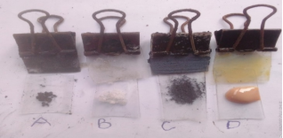
Figure 1. Samples and the thin films Carbon (A), CuAlSe2 (B), Coal (C) and TiO2 doped with RGO (D) TiO2 on FTO glass substrate (solaronix).
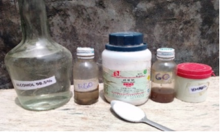
Figure 2. Starting materials and the thin films carbon, TiO2 on FTO glass substrate.
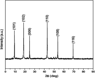
Figure 3. X-ray diffraction pattern of CuInSe2.
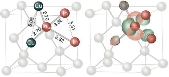
Figure 4. The interatomic distances in A0 around defect atom in CuInSe2 [18].
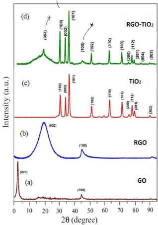
Figure 5. XRD Analysis of the RGO-TiO2, RGO, GO on quartz substrate.
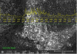
Figure 6. SEM micrograph of samples RGO-CuAlSe2-TiO2 at magnification of 250x.
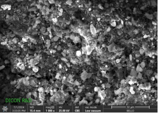
Figure 7. SEM micrograph of samples RGO-CuAlSe2-TiO2 at magnification of 1000x.
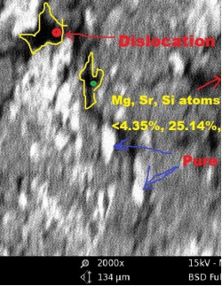
Figure 8. (a) Crystal defects in RGO-CuAlSe2-TiO2.
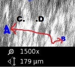
Figure 9. Continuity test and electrical continuity point A to B.
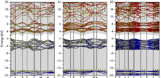
Figure 10. TiO2 band-structures: Rutile, Anatase and-brookite .
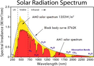
Figure 11. Solar Energy Spectrum.
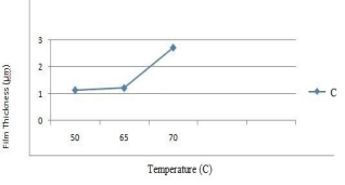
Figure 12. A graph of film thickness versus the deposition temperature.
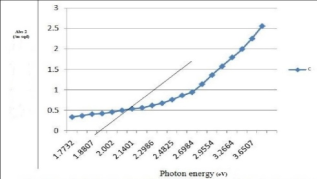
Figure 13. Absorption coefficient squared x 1012 (/m2) versus photon energy for C at 600C.
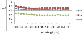
Figure 14. The transmittance versus wavelength (nm) of the radiation.
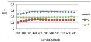
Figure 15. The reflectance versus wavelength (nm) of the radiation.
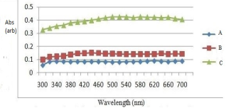
Figure 16. Absorbance versus wavelengths sample A, B and C.
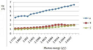
Figure 17. Optical conductivity against photo energy of samples A, B and C.
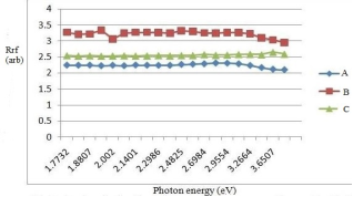
Figure 18. Refractive index of the samples against the photon energy.
Information