Research Article | | Peer-Reviewed

Comparative Performance Analysis of RC-Coupled, Transformer-Coupled, and Direct-Coupled Common-Emitter Transistor Amplifiers Using Multisim 11.0

Received: 15 July 2026     Accepted: 25 July 2026     Published: 9 September 2026
Views:       Downloads:
Abstract

The coupling technique employed in multistage transistor amplifiers plays a fundamental role in determining voltage gain, frequency response, bandwidth, and overall amplifier performance. Although resistance-capacitance (RC), transformer, and direct coupling are widely used in analog electronic systems, their comparative performance under identical operating conditions has not been comprehensively investigated. This study aimed to compare the performance of two-stage RC-coupled, transformer-coupled, and direct-coupled common-emitter transistor amplifiers using Multisim 11.0. Three amplifier configurations were designed using identical circuit parameters, including two 2N2222A NPN transistors, a 12 V DC supply, identical voltage-divider bias networks, collector and emitter resistors, and the same input signal conditions. The only difference among the circuits was the interstage coupling technique. Simulations were carried out over a frequency range of 10 Hz to 100 MHz, and the amplifiers were evaluated in terms of voltage gain, frequency response, bandwidth, waveform characteristics, phase relationship, and signal amplification behaviors. The simulation results showed that the RC-coupled amplifier exhibited the highest and most stable mid-band voltage gain of approximately 68 dB together with the widest useful bandwidth, making it the most suitable for general-purpose voltage amplification. The transformer-coupled amplifier demonstrated moderate performance with a peak gain around 100 kHz, indicating its suitability for impedance matching and efficient power transfer. The direct-coupled amplifier produced the lowest voltage gain under the selected operating conditions but retained the capability to amplify DC and very low-frequency signals because it does not employ coupling capacitors or transformers. The study concludes that the choice of coupling technique significantly influences transistor amplifier performance. RC coupling is the preferred technique for high-gain, wide-band voltage amplification, transformer coupling is advantageous for impedance matching and power amplification, whereas direct coupling is most suitable for DC and low-frequency instrumentation applications. These findings provide practical guidance for selecting appropriate coupling techniques in the design of multistage transistor amplifiers.

Published in Journal of Electrical and Electronic Engineering (Volume 14, Issue 4)
DOI 10.11648/j.jeee.20261404.12
Page(s) 196-210
Creative Commons

This is an Open Access article, distributed under the terms of the Creative Commons Attribution 4.0 International License (http://creativecommons.org/licenses/by/4.0/), which permits unrestricted use, distribution and reproduction in any medium or format, provided the original work is properly cited.

Copyright

Copyright © The Author(s), 2026. Published by Science Publishing Group

Keywords

Common-Emitter Amplifier, RC Coupling, Transformer Coupling, Direct Coupling, Frequency Response, Voltage Gain, Multisim

1. Introduction
Transistor amplifiers are fundamental components of analog electronic systems and play a vital role in communication systems, instrumentation, biomedical devices, industrial control, and consumer electronics. Their primary function is to amplify weak electrical signals while preserving the signal waveform with minimum distortion . Among the various transistor amplifier configurations, the common-emitter (CE) amplifier is the most widely used because it provides high voltage gain, moderate input impedance, and satisfactory frequency response, making it suitable for both voltage and power amplification applications . In many practical applications, however, a single transistor stage cannot provide sufficient gain to meet system requirements. Consequently, two or more amplifier stages are connected in cascade to form multistage amplifiers, where the method of coupling successive stages significantly influences voltage gain, bandwidth, impedance matching, frequency response, and overall amplifier performance .
Among the commonly used interstage coupling techniques are resistance-capacitance (RC) coupling, transformer coupling, and direct coupling. RC coupling is the most widely adopted technique in audio-frequency and low-power voltage amplifiers because of its simple circuit design, low cost, and relatively flat mid-band frequency response. However, the coupling and bypass capacitors introduce attenuation at low frequencies, while transistor junction capacitances limit high-frequency performance . Transformer coupling offers superior impedance matching and efficient power transfer, making it suitable for power amplifiers and impedance-sensitive circuits. Nevertheless, transformer-coupled amplifiers generally exhibit reduced bandwidth, increased size, and frequency-dependent characteristics due to transformer inductance and leakage effects . Direct coupling eliminates coupling capacitors and transformers, thereby enabling the amplification of both direct-current (DC) and very low-frequency signals. Although this technique is widely used in operational amplifiers and instrumentation systems, it requires careful bias stabilization because of temperature-induced drift and transistor parameter variations .
Several researchers have investigated transistor amplifier performance using theoretical analysis, mathematical modelling, experimental measurements, and circuit simulation. developed a design theory for balanced transistor amplifiers and demonstrated improved gain stability and impedance matching in high-frequency amplifier circuits. experimentally investigated the frequency response of bipolar junction transistor amplifiers and reported that collector resistance, load resistance, and operating frequency significantly influence amplifier gain and bandwidth. Although these studies improved the understanding of transistor amplifier characteristics, they focused primarily on amplifier configurations rather than the influence of coupling methods.
Recent studies have further advanced transistor amplifier analysis. investigated the effect of transistor non-linearity on common-emitter amplifier performance and showed that transistor parameters significantly influence voltage gain and signal linearity. proposed generalized analytical expressions for gain and impedance in single-transistor amplifiers, providing a unified mathematical framework for amplifier design. simulated common-emitter and Darlington transistor amplifiers and compared their voltage gain, current gain, bandwidth, and power dissipation, concluding that Darlington amplifiers provide higher current gain than conventional common-emitter amplifiers. However, the study focused on transistor configurations instead of comparing different coupling techniques.
Other studies have concentrated on specific coupling methods. reported that RC-coupled amplifiers provide stable voltage gain and excellent audio-frequency performance, making them the preferred choice for small-signal amplification. explained that transformer-coupled amplifiers provide improved impedance matching and higher power transfer efficiency but suffer from limited frequency response due to transformer characteristics. highlighted that direct-coupled amplifiers are particularly suitable for low-frequency and DC applications but require careful bias stabilization to minimize drift and offset errors. Similarly, emphasized that amplifier performance depends not only on transistor characteristics but also on component selection, bias stability, and circuit topology. further demonstrated that proper bias design and operating-point selection are essential for achieving stable amplifier operation and minimizing signal distortion.
Despite these significant contributions, most previous investigations have focused on a single coupling technique, theoretical analysis, or comparisons between different transistor configurations. Very few studies have presented a systematic comparison of RC-coupled, transformer-coupled, and direct-coupled common-emitter transistor amplifiers designed under identical operating conditions using the same transistor type, power supply, biasing network, and load resistance. Consequently, the individual influence of the coupling technique on amplifier gain, frequency response, bandwidth, waveform characteristics, and overall performance has not been comprehensively investigated under comparable conditions.
To address this gap, the present study designs and simulates two-stage RC-coupled, transformer-coupled, and direct-coupled common-emitter transistor amplifiers using Multisim 11.0 under identical operating conditions. Each amplifier employs the same 2N2222A transistor, supply voltage, biasing arrangement, and component values to ensure a fair comparison. The amplifier performances are evaluated in terms of voltage gain, frequency response, bandwidth, waveform characteristics, and signal amplification behaviors. The findings are expected to provide practical guidance for amplifier designers, researchers, and engineering students in selecting the most appropriate coupling technique for specific analog electronic applications while contributing to the understanding of multistage transistor amplifier performance.
2. Methodology
The methodology adopted in this study involved the design, simulation and comparative performance evaluation of two-stage RC-coupled, transformer-coupled and direct-coupled transistor amplifiers using Multisim 11.0. Three separate amplifier circuits were designed under identical operating conditions so that the effect of the coupling technique on amplifier performance could be investigated. The comparison was based on voltage gain, frequency response, bandwidth, phase relationship, waveform distortion and DC bias stability.
2.1. Circuit Design
The design of each transistor amplifier was carried out by determining the appropriate values of the following circuit parameters:
1) Supply voltage (VCC)
2) DC operating point (Q-point)
3) Collector and emitter resistors (RCandRE)
4) Base bias resistors (R1and R2)
5) Source resistance (Rg)
6) Coupling, bypass and output capacitors
7) Complete circuit configuration
The design procedure adopted in this study follows the standard transistor amplifier design approach described by .
(VCC)2.1.1. Selection of the Supply Voltage
The supply voltage must be selected such that it does not exceed the maximum collector-emitter voltage rating of the transistor. According to the datasheet of the 2N2222A NPN transistor, the maximum collector-emitter voltage (VCEO) is 40 V . Therefore, considering safe operating conditions, ease of implementation and laboratory availability, a supply voltage of 12V was selected for the design.
VCC=12V(1)
2.1.2. Selection of the Operating Point (Q-Point)
The operating point (Q-point) represents the steady-state DC operating conditions of the transistor and is defined by the collector current (IC), base current (IB) and collector-emitter voltage (IE) . A properly selected operating point ensures that the transistor operates within the active region, thereby providing maximum undistorted signal amplification . The base current is determined from:
IB= ICβ(2)
were
1) IC = collector current,
2) IB = base current,
3) β = DC current gain of the transistor.
To obtain symmetrical output signal swing with minimum distortion, the collector-emitter voltage should satisfy :
VCC3<VCE<VCC2(3)
For the selected supply voltage, VCC=12V the lower limit of the operating range becomes VCE=123=4V
A collector current of IC=4mA was selected as the design operating current. Assuming a transistor current gain of β = 200 the corresponding base current is:
IB=4×10-3200
IB=2×10⁻⁵A
IB=20μA
Therefore,
1) Collector-emitter voltage, VCE=4V
2) Collector current, IC=4mA
3) Base current, IB=20μA
constitute the selected DC operating point (Q-point) for the amplifier design. This operating point provides sufficient collector-emitter voltage to allow symmetrical amplification of the input signal while minimizing output waveform distortion.
2.1.3. Selection of the Collector and Emitter Resistors
The collector resistor (RC) and emitter resistor (RE) were selected to establish the desired DC operating point while ensuring stable transistor operation. For a common-emitter amplifier, it is generally assumed that the emitter current is approximately equal to the collector current . that is,
ICIE(4)
Furthermore, for symmetrical voltage swing and good thermal stability, the collector and emitter resistors are commonly chosen to have approximately equal values . Applying Kirchhoff's Voltage Law (KVL) to the collector-emitter loop gives:
VCC=ICRC+VCE+IERE(5)
Since, ICIE and RCRE
Equation (5) can be simplified to
VCC=ICRC+RE+VCE
Hence,RC=VCC - VCE2IC(6)
Substituting the selected design values,
VCC=12V,  VCE=4V,  IC=4mA
Gives, RC=12-42×4×10-3
RC=80.008=1000Ω=1, Since, RERC
Thus, the selected resistor values for the amplifier design are:
RC=RE=1
These resistor values establish the required operating point, provide adequate voltage drop across both the collector and emitter resistors, and improve thermal stability while allowing sufficient collector-emitter voltage for undistorted signal amplification.
2.1.4. Selection of the Bias Resistors (R1 and R2)
The bias resistors R1 and R2 form the voltage-divider bias network, which establishes the required base voltage and ensures stable operation of the transistor . A properly designed voltage-divider bias minimizes the influence of transistor current gain (β) variations and improves thermal stability. Applying Kirchhoff's Voltage Law (KVL) to the base-emitter loop gives:
I2R2=VBE+VE(7)
were
1) I2 = current flowing through R2,
2) VBE = base-emitter voltage,
3) VE = emitter voltage
The emitter voltage is obtained from, VE=VCC-VCE
Substituting the selected design values, Ve=12-4=8V
Assuming a silicon transistor, VBE=0.6V
Therefore, I2R2=0.6+8=8.6V
Applying KVL to the voltage-divider network gives: VCC-R1I1-VBE-VE=0
Were, I1=(I2+IB)
Therefore,R1=Vcc-VBE(I2+IB)(8)
To ensure that the transistor base current has negligible effect on the voltage-divider network, the divider current is selected to be much greater than the base current. A commonly accepted design practice is: I210IB .
In this study, I2 = 25 × IB, was selected to provide improved bias stability.
Since, IB=20μA, then, I2 = 25 × IB, = 25 × 0.00002 = 0.0005A = 0.5mA
Because, IBI2, the base current can be neglected in Equation (8), giving
R1=12 - 0.60.0005=11.60.0005= 22800 Ω = 22.8k Ω andR2=8.60.0005= 17200Ω = 17.2kΩ
Similarly, R2=8.6I2=8.65×10-3=17200Ω=17.2
Therefore, the selected bias resistor values are: R1 = 22.8 k Ω and R2 = 17.2k Ω
These resistor values establish the required base bias voltage, maintain the transistor in the active region, and improve the stability of the operating point against variations in transistor current gain and temperature.
(Rg)2.1.5. Selection of the Source Resistance
The source resistance (Rg) represents the internal resistance of the signal source supplying the input AC signal to the amplifier . The value of Rg influences the input current and, consequently, the voltage gain of the amplifier. According to Ohm's law, the AC emitter current is given by .
ie=VinputRg(9)
were
1) ie = AC emitter current,
2) Vinput = input AC voltage,
3) Rg= source resistance.
For a common-emitter transistor amplifier operating in the active region, the AC collector current is approximately equal to the AC emitter current. Hence
ieic(10)
The output AC voltage developed across the collector resistor is therefore
Voutput=icRc=ieRc(11)
Substituting Equation (9) into Equation (11) gives
Voutput=RcRgVinput(12)
The small-signal voltage gain of the amplifier is defined as
AV=VoutVin(13)
Substituting Equation (12) into Equation (13) yields
AV=RCRg
Hence, the required source resistance for a specified voltage gain can be expressed as
Rg=RCRg(14)
Equation (14) provides the theoretical relationship between the collector resistance, source resistance and voltage gain. In the present work, however, the input signal was supplied by the Multisim function generator, whose internal output resistance remained fixed throughout the simulations. Consequently, the input signal amplitude was maintained at 10 mVP for all simulations, and Rg was not varied during the comparative analysis.
2.1.6. Selection of the Capacitors
The coupling and bypass capacitors were selected to ensure efficient transmission of AC signals while maintaining the required DC operating conditions of the amplifier. The input and output coupling capacitors block DC components between amplifier stages while allowing AC signals to pass, whereas the emitter bypass capacitor provides a low-reactance path for AC signals around the emitter resistor, thereby increasing the voltage gain .
(Cin)(i) Selection of the Input Coupling Capacitor
The input coupling capacitor and the input resistance of the amplifier form a high-pass RC network, the voltage across the resistor is given by .
VR=RR2+1ω2c2Vinput(15)
were
1) R=R2
2) C=Cin
3) ω=2πf
f is the input signal frequency.
For audio-frequency amplifier design, the lowest operating frequency was selected as, f = 20Hz , to establish the lower cut-off frequency, the capacitor was selected such that the output voltage across the resistor is one-half of the input voltage.
Therefore,VRVin=12(16)
Substituting Equation (16) into Equation (15) gives
Cin=13R22ω2
Were, ω=2πf=2×3.142×20=123.68rad/s
Substituting, R2=17.2,
gives Cin=2.67×10⁻⁷F=0.267μF,
was selected as the input coupling capacitor.
(Cout)(ii) Selection of the Output Coupling Capacitor
The output coupling capacitor was determined using the same design approach. The voltage across the load resistor is
VR=RR2+1ω2c2Vout(17)
At the lower cut-off frequency,
VRVout=12
Therefore, Cout=13RC2ω2
Using, RC=1000Ω and ω=125.68rad/s,
gives, Cout=4.59×10-6=4.5μF
was selected as the output coupling capacitor.
(CE)(iii) Selection of the Emitter Bypass Capacitor
The emitter bypass capacitor provides a low-reactance path for AC signals around the emitter resistor, thereby reducing AC negative feedback and increasing the voltage gain of the amplifier. The capacitor value was determined from the RC time constant relationship,
T = RC(18)
Were, T=1f
At the lowest operating frequency, f = 20Hz
Therefore, T=120=0.05s
Hence, CE=TRE
Substituting, RE=1000Ω
gives CE=0.051000=5×10⁻⁵F=50μF
was selected as the emitter bypass capacitor
2.2. Design of the Two-Stage RC-Coupled Common-Emitter Transistor Amplifier
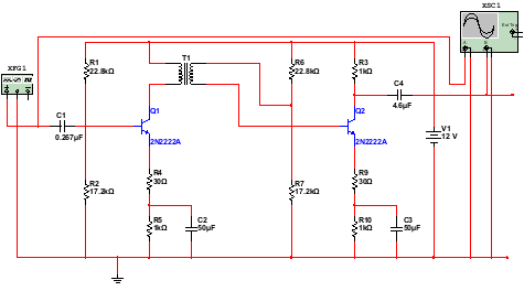
Based on the design calculations presented in Sections 2.1.1–2.1.6, the component values required for the two-stage RC-coupled common-emitter transistor amplifier were determined and implemented in Multisim 11.0. The amplifier was designed using two 2N2222A NPN transistors operating in the active region and powered by a 12 V DC supply. The selected component values are:
1) Supply voltage, VCC=12V
2) Collector resistor, RC=1
3) Emitter resistor, RE=1
4) Upper bias resistor, R1=22.8
5) Lower bias resistor, R2=7.2
6) Input coupling capacitor, Cin=0.267μF
7) Output coupling capacitor, Cout=4.59μF
8) Emitter bypass capacitor, CE=50μF
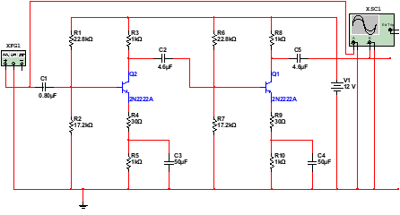
The amplifier consists of two common-emitter transistor stages interconnected through RC coupling. The coupling capacitor transfers the amplified AC signal from the first stage to the second stage while blocking the DC component, thereby preserving the biasing conditions of each stage. The voltage-divider bias network was employed to establish a stable operating point for both transistors, while the emitter bypass capacitor was included to improve AC voltage gain by reducing emitter degeneration. The complete circuit was implemented and simulated in Multisim 11.0, where identical component values were used in both amplifier stages to ensure consistent operating conditions. The completed schematic of the two-stage RC-coupled common-emitter transistor amplifier is shown in Figure 1.
Figure 1. Multisim 11.0 schematic of the designed two-stage RC-coupled common-emitter transistor amplifier.
2.3. Design of the Two-Stage Transformer-Coupled Common-Emitter Transistor Amplifier
To ensure a meaningful comparison between the RC-coupled, transformer-coupled, and direct-coupled transistor amplifiers, all three amplifier configurations were designed to operate under identical DC operating conditions. Consequently, the same transistor type (2N2222A), supply voltage (VCC=12V), voltage-divider bias network, collector current, emitter current, and emitter resistor values determined for the RC-coupled amplifier were retained in the transformer-coupled design. The only modification was the replacement of the interstage RC coupling network with an interstage transformer. In the transformer-coupled amplifier, the collector resistor (RC=1) of the first stage was replaced by the primary winding of the transformer, while the interstage coupling capacitor (Cout=4.59 μF) was replaced by the transformer itself. The voltage-divider bias network and all other circuit components remained unchanged to ensure that any variation in amplifier performance resulted solely from the coupling method.
2.3.1. Determination of the Transformer Primary Inductance
The collector resistor being replaced has a value of RC=1000Ω, for the transformer to provide effective AC coupling without significantly loading the collector circuit, the inductive reactance of the primary winding should be much greater than the collector resistance at the chosen reference frequency. A commonly adopted design criterion is
XL10RC
Therefore, XL=10×1000=10000Ω
The inductive reactance of the primary winding is given by
XL=2πfLP(19)
were
1) XL = inductive reactance, 6
2) f = operating frequency,
3) LP = primary inductance.
Using the reference frequency, f = 1kHz,
the required primary inductance is LP=XL2πf
Substituting the design values,
Lp=100002π(1000)
Lp=10006283
Lp1.59H
Therefore, Lp1.59H was selected as the transformer primary inductance.
2.3.2. Determination of the Secondary Inductance
A 1:1 turns ratio was selected to allow the transformer to transfer the amplified signal between stages without introducing either voltage step-up or voltage step-down. The relationship between the primary and secondary inductances is given by
LPLS=NPNS2
where:
1) LP = primary inductance (H)
2) LS = secondary inductance (H)
3) NP = number of primary turns
4) NS = number of secondary turns
Since the selected turns ratio is Np:Ns=1:1, then Lp=Ls
Therefore, Ls=1.6H.
2.3.3. Determination of the Coupling Coefficient
The coupling coefficient (k) indicates the magnetic coupling efficiency between the primary and secondary windings. For a practical transformer, values between 0.98 and 0.99 represent very good magnetic coupling with minimal leakage flux .
In this work, k = 0.99
was selected to represent an almost ideal transformer suitable for simulation. The transformer therefore replaces both:
1) the collector resistor (RC=1 kΩ), and
2) the interstage coupling capacitor (CC=4.59 μF).
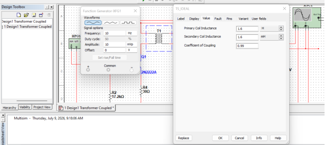
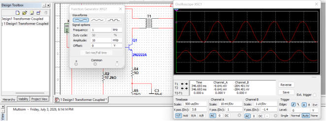
Using a primary inductance of 1.6 H provides an inductive reactance of approximately 10 kΩ at the design frequency of 1 kHz, thereby enabling the transformer-coupled amplifier to operate under conditions comparable to those of the RC-coupled amplifier. The complete circuit diagram of the two-stage transformer-coupled common-emitter transistor amplifier is shown in Figure 2, while Figure 3 illustrates the transformer properties and simulation settings. The transformer parameters used in the simulation are:
1) Primary inductance (LP) = 1.6 H
2) Secondary inductance (LS) = 1.6 H
3) Coupling coefficient (k) = 0.99
4) Turns ratio (NP:NS) = 1:1
For the transient simulation, an input signal with an amplitude of 10 mV, a DC offset of 0 V, and a frequency of 10 Hz was applied. Although the transformer was designed based on a 1 kHz operating frequency, using 10 Hz during simulation enables the low-frequency response of the amplifier to be investigated. Additional simulations may also be performed at 1 kHz to evaluate the amplifier under its design operating condition.
Figure 2. Complete circuit diagram of the two-stage transformer-coupled common-emitter transistor amplifier.
Figure 3. Illustrates the transformer properties and simulation settings.
2.4. Common Emitter Transistor Amplifier Design for Direct Coupling
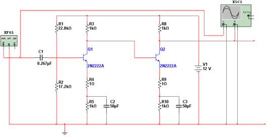
To ensure a fair comparison with the RC-coupled and transformer-coupled amplifier configurations, the direct-coupled amplifier was designed using the same transistor type, power supply voltage, and DC biasing conditions. This approach ensures that the differences observed in amplifier performance are attributed solely to the coupling method rather than changes in the circuit operating conditions. In the direct-coupled amplifier configuration, the interstage coupling capacitor used in the RC-coupled amplifier and the transformer used in the transformer-coupled amplifier are eliminated. Instead, the collector of the first transistor stage is connected directly to the base of the second transistor stage, allowing both the AC signal and the DC bias voltage to be transferred directly between stages. The biasing network was appropriately adjusted where necessary to maintain the required operating point of the second transistor while preserving stable amplifier operation. The complete circuit diagram of the two-stage direct-coupled common-emitter transistor amplifier is shown in Figure 4. The amplifier employs the same transistor type, supply voltage, and component values as the other amplifier configurations, except for the removal of the coupling capacitor and transformer. This configuration enables a direct comparison of voltage gain, frequency response, and signal amplification characteristics with the RC-coupled and transformer-coupled amplifiers under identical operating conditions.
Figure 4. Complete circuit diagram of the two-stage direct-coupled common-emitter transistor amplifier
3. Simulation Procedure for RC, Transformer and Direct-Coupled Amplifiers
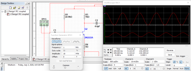
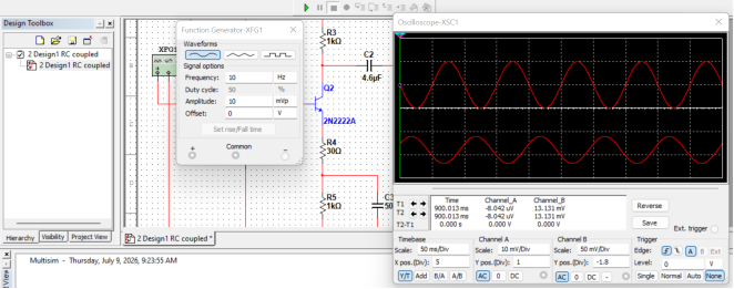
The purpose of the simulation was to evaluate and compare the performance of the designed two-stage RC-coupled, transformer-coupled and direct-coupled transistor amplifiers under identical operating conditions using Multisim 11.0. The comparison was based on voltage gain, output waveform, frequency response, bandwidth, phase relationship and waveform distortion. After completing the design of each amplifier circuit, all component values and circuit connections were verified before the simulation was carried out. Each amplifier circuit was designed using identical components, comprising two 2N2222A NPN transistors, a 12 V DC power supply, identical bias resistor values, identical collector and emitter resistor values, identical input signal conditions and the same measuring instruments. The only difference among the three amplifier circuits was the coupling technique employed between the two amplification stages, namely RC coupling, transformer coupling and direct coupling. The simulation was performed by clicking the Run button in Multisim 11.0. The input and output waveforms were monitored simultaneously using the two-channel oscilloscope. Before taking any measurements, the amplifier output was observed to ensure that the transistor stages were correctly biased and that the output waveform remained stable without excessive clipping or distortion. The simulated oscilloscope displays for the RC-coupled, transformer-coupled and direct-coupled amplifiers are presented in Figures 5, 6 and 7, respectively.
Figure 5. RC-coupled amplifier input and output waveforms displayed on the oscilloscope.
Figure 6. Transformer coupled input and output waveforms displayed on the oscilloscope.
Figure 7. Direct coupled input and output waveforms displayed on the oscilloscope.
A sinusoidal input signal having a constant peak amplitude of 10 mV was generated using the Multisim function generator. The input frequency was varied from 10 Hz to 100 MHz while maintaining the input amplitude constant throughout the simulation. At each selected frequency, the input voltage was measured using Channel A of the oscilloscope, while the output voltage was measured using Channel B. The peak voltage was obtained by counting the number of vertical divisions occupied by the waveform from the highest peak to the lowest trough and multiplying by the channel sensitivity before dividing by two. The peak voltage was therefore determined using Equation (19).
Vp=Number of Vertical Divisions×Channel Scale2(19)
The voltage gain of each amplifier was calculated using Equation (20).
Av=Vout(p)Vin(p)(20)
Converting voltage gain to decibels (dB) will produce a professional Bode magnitude plot, which is the standard format used in electronics journals, the conversion is:
AV(dB)=20log10(AV)(21)
The RC-coupled amplifier was first simulated at an input frequency of 10 Hz using a sinusoidal input signal having a peak amplitude of 10 mV. The input and output waveforms were displayed simultaneously on the oscilloscope as shown in Figure 7. For the input signal, Channel A was set to 10 mV/div. The waveform occupied approximately 2 vertical divisions from peak to trough. Applying Equation (19),
Vin(p)=2×10mV2=10mV
For the output signal, Channel B was set to 50 mV/div. The output waveform occupied approximately 10 vertical divisions from peak to trough. Therefore,
Vout(p)=10×50mV2=250mV
Substituting these values into Equation (20),
AV=250mV10mV =25
The voltage gain in decibel is:
AV=20log10(25)=27.96dB
Hence, the voltage gain of the RC-coupled amplifier at 10 Hz was 25 which is 27.96dB.
The same measurement procedure was repeated for the transformer-coupled and direct-coupled amplifiers at all selected frequencies between 10 Hz and 100 MHz while maintaining the input signal at 10 mVp. The measured output voltages were used to calculate the corresponding voltage gains, and the results were recorded in Table 1 and Table 2 is the converted table based on simulation results. These results formed the basis for comparing the gain characteristics, frequency response, bandwidth, low-cut frequency, high-cut frequency, waveform distortion and phase relationship of the three amplifier coupling techniques.
Figure 7. RC coupled input and output waveforms displayed on the oscilloscope.
Table 1. Simulation Data for Comparative Analysis of the Three Amplifier

Frequency

Input VP (mV)

RC Output VP (mV)

RC Gain (Av)

Transformer Output VP (mV)

Transformer Gain (Av)

Direct Output VP (mV)

Direct Gain (Av)

10Hz

10

250

25

0.00005

0.000005

0.0000025

0.00000025

15Hz

10

600

60

0.0001

0.00001

0.0000125

0.00000125

100Hz

10

15,000

1,500

0.00025

0.000025

0.000025

0.0000025

200Hz

10

25,000

2,500

0.0009

0.00009

0.000015

0.0000015

500Hz

10

25,000

2,500

0.0015

0.00015

0.000009

0.0000009

1kHz

10

25,000

2,500

0.003

0.0003

0.0000045

0.000000045

10KHz

10

25,000

2,500

0.24

0.024

0.00003

0.000003

100KHz

10

25,000

2,500

150

15

0.0003

0.00003

1MHz

10

22,500

2,250

9.5

0.95

0.004

0.0004

10MHz

10

7,500

750

2.5

0.25

0.045

0.0045

20MHz

10

4,500

450

1

0.1

0.09

0.009

100MHz

10

750

75

0.03

0.003

0.45

0.045

Table 2. Comparison of voltage gain in decibels (dB) of RC-coupled, transformer-coupled, and direct-coupled common-emitter amplifiers over the simulated frequency range.

Frequency (Hz)

RC Gain (dB)

Transformer Gain (dB)

Direct Gain (dB)

10

27.96

-106.02

-132.04

15

35.56

-100.00

-118.06

100

63.52

-92.04

-112.04

200

67.96

-80.92

-116.48

500

67.96

-76.48

-120.92

1,000

67.96

-70.46

-126.94

10,000

67.96

-32.40

-110.46

100,000

67.96

23.52

-90.46

1,000,000

67.04

-0.45

-67.96

10,000,000

57.50

-12.04

-46.94

20,000,000

53.06

-20.00

-40.92

100,000,000

37.50

-50.46

-26.94

4. Results and Discussions
The performance of the designed two-stage RC-coupled, transformer-coupled, and direct-coupled transistor amplifiers was evaluated using Multisim 11.0 under identical operating conditions. Each amplifier employed two 2N2222A NPN transistors, a 12 V DC power supply, identical biasing networks, collector and emitter resistor values, and the same sinusoidal input signal. The only difference among the three amplifier circuits was the coupling technique used between successive transistor stages. The simulation results were analyzed based on voltage gain, frequency response, bandwidth, waveform characteristics, phase relationship, and signal distortion.
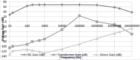
Figure 8. Frequency response of RC-, transformer-, and direct-coupled transistor amplifiers.
The RC-coupled amplifier exhibited the best overall frequency response among the three amplifier configurations.
4.1. Comparative Frequency Response of the Three Amplifier Configurations
As shown in Figure 8, the voltage gain increased from approximately 28 dB at 10 Hz to about 68 dB within the mid-frequency region (approximately 200 Hz to 1 MHz), where it remained relatively constant. Beyond this range, the gain gradually decreased to approximately 38 dB at 100 MHz This behavior is characteristic of RC-coupled amplifiers, which exhibit a nearly flat mid-band response with attenuation occurring at both low and high frequencies. The reduced gain at low frequencies is primarily due to the large reactance of the coupling and emitter-bypass capacitors, whereas the gain reduction at high frequencies results from transistor junction capacitances and other parasitic effects. These observations are consistent with the findings of and , who reported that RC-coupled amplifiers provide high voltage gain, wide bandwidth, and excellent frequency response, making them suitable for voltage amplification applications.
The transformer-coupled amplifier demonstrated a frequency-dependent response with significantly lower gain than the RC-coupled amplifier. At low frequencies, the gain remained below −100 dB, indicating poor signal transfer due to the low inductive reactance of the transformer primary winding. As the frequency increased, the gain improved steadily and reached a maximum value of approximately 24 dB at around 100 kHz. Beyond this frequency, the gain decreased progressively, reaching approximately −50 dB at 100 MHz This behavior reflects the inherent limitations of transformer coupling, where leakage inductance, winding resistance, inter-winding capacitance, and core losses become increasingly significant at higher frequencies. Although transformer-coupled amplifiers generally exhibit poorer frequency response than RC-coupled amplifiers, they remain advantageous for impedance matching and power transfer, as reported by .
The direct-coupled amplifier produced the lowest gain throughout most of the investigated frequency range. The simulated gain was approximately −132 dB at 10 Hz and increased gradually with frequency to about −27 dB at 100 MHz Although the amplifier exhibited lower voltage gain than the other configurations, this result does not diminish the principal advantage of direct coupling. Unlike RC- and transformer-coupled amplifiers, direct-coupled amplifiers do not employ coupling capacitors or transformers and are therefore capable of amplifying direct current (DC) and extremely low-frequency signals without low-frequency attenuation. Consequently, they are widely used in operational amplifiers, instrumentation amplifiers, biomedical electronics, and precision measurement systems. The relatively low gain observed in the present simulation is likely attributable to the selected transistor bias conditions and operating point rather than to the direct-coupling technique itself.
Overall, the simulation results demonstrate that the coupling technique has a significant influence on amplifier performance. Among the three amplifier configurations, the RC-coupled amplifier achieved the highest and most stable mid-band gain (approximately 68 dB) together with the widest useful bandwidth. The transformer-coupled amplifier exhibited a pronounced peak around 100 kHz, reflecting its frequency-selective characteristics, while the direct-coupled amplifier maintained comparatively low gain across the investigated frequency range but showed gradual improvement at higher frequencies. These findings confirm that RC coupling is the most suitable technique for general-purpose voltage amplification, transformer coupling is preferable for impedance matching and power transfer applications, and direct coupling is most appropriate for DC and very low-frequency signal amplification.
4.2. Comparison of Simulation Results with Theoretical Expectations
The simulation results obtained in this investigation generally agree with the established theoretical characteristics of the three amplifier coupling techniques, although some deviations were observed for the transformer-coupled and direct-coupled amplifier configurations.
The RC-coupled amplifier closely followed the expected theoretical behaviors by providing the highest voltage gain and maintaining a nearly constant gain throughout the mid-frequency region before decreasing at both low and high frequencies, as illustrated in Figure 8. This agrees with the work of and , who reported that RC-coupled amplifiers exhibit excellent frequency response and are widely used for voltage amplification in audio and communication systems because of their high gain and broad bandwidth.
The transformer-coupled amplifier produced considerably lower gain than predicted by ideal theoretical analysis. Although transformer coupling is widely recognized for impedance matching and efficient power transfer, its performance depends strongly on transformer parameters such as primary and secondary inductance, leakage inductance, winding resistance, coupling coefficient, and core characteristics. The peak gain observed near 100 kHz suggests that the selected transformer parameters were most effective around this operating frequency, while the reduced gain at lower and higher frequencies reflects practical transformer limitations.
Similarly, the direct-coupled amplifier produced substantially lower gain than expected from theory. According to and , the principal advantage of direct coupling lies in its ability to amplify DC and extremely low-frequency signals without attenuation caused by coupling capacitors or transformers. Therefore, direct-coupled amplifiers are primarily intended for instrumentation, control systems, and precision measurement applications rather than high-gain, wideband voltage amplification. The low gain obtained during the present simulation is therefore more likely associated with the selected bias conditions, transistor operating points, and circuit implementation than with the direct-coupling technique itself.
The differences observed between the simulated and theoretical characteristics demonstrate the importance of practical circuit design. Theoretical analyses generally assume ideal components and perfectly established operating conditions, whereas practical simulations incorporate realistic transistor models, transformer non-idealities, parasitic capacitances, and component tolerances. Consequently, some deviations between theoretical predictions and simulated performance are expected and do not invalidate the fundamental operating principles of the three coupling techniques.
Overall, the comparative analysis confirms that RC coupling provides the highest voltage gain, the widest useful bandwidth, and the most stable frequency response, making it the preferred choice for general-purpose voltage amplification. Transformer coupling remains advantageous for impedance matching and efficient power transfer, while direct coupling is best suited for DC and very low-frequency amplification when appropriate bias stabilization and temperature compensation are employed.
5. Conclusion
This study compared the performance of two-stage RC-coupled, transformer-coupled, and direct-coupled common-emitter transistor amplifiers using Multisim 11.0 under identical operating conditions. The results showed that the RC-coupled amplifier achieved the highest voltage gain (approximately 68 dB), the widest useful bandwidth, and the most stable frequency response, making it the most suitable for general-purpose voltage amplification. The transformer-coupled amplifier exhibited moderate gain with peak performance around 100 kHz, making it suitable for impedance matching and power transfer applications. Although the direct-coupled amplifier produced the lowest voltage gain under the selected design conditions, it remains advantageous for amplifying DC and very low-frequency signals. Overall, the study confirms that the choice of coupling technique significantly influences amplifier performance and should be selected according to the intended application. The findings provide useful guidance for the design and implementation of multistage transistor amplifiers in analog electronic systems.
Abbreviations

AC

Alternating Current

BJT

Bipolar Junction Transistor

CE

Common Emitter

DC

Direct Current

RC

Resistor-Capacitor

VCC

Collector Supply Voltage

VCE

Collector-Emitter Voltage

VBE

Base-Emitter Voltage

IC

Collector Current

IB

Base Current

IE

Emitter Current

β (Beta)

DC Current Gain of the Transistor

Av

Voltage Gain

Zin

Input Impedance

Zout

Output Impedance

BW

Bandwidth

fL

Lower Cutoff Frequency

fH

Upper Cutoff Frequency

Hz

Hertz

kHz

Kilohertz

MHz

Megahertz

mV

Millivolt

V

Volt

mA

Milliampere

Ω

Ohm

Kilo-ohm

μF

Microfarad

nF

Nanofarad

pF

Picofarad

NPN

Negative-Positive-Negative Bipolar Transistor

Q

Transistor Designator (e.g., Q1)

R

Resistor

C

Capacitor

Vin

Input Voltage

Vout

Output Voltage

Vpp

Peak-to-Peak Voltage

XFG1

Function Generator Instrument in Multisim

XSC1

Oscilloscope Instrument in Multisim

Author Contributions
Yusuf Abdullahi: Conceptualization, Methodology, Software, Investigation, Formal Analysis, Validation, Visualization, Writing – original draft, Writing – review & editing
Ismail Garba Saidu: Methodology, Supervision, Validation, Writing – review & editing
Muhammad Bello Abdullahi: Data Curation, Investigation, Validation, Writing – review & editing
Kabiru Ahmed Dabai: Resources, Validation, Writing – review & editing
Buhari Bello Sahabi: Formal Analysis, Visualization, Validation, Writing – review & editing
Aisha Aminu Mode: Resources, Supervision, Writing – review & editing
Conflicts of Interest
The authors declare no conflicts of interest.
References
[1] Abdullahi, Y., & Sahabi, B.(2019). Design and Simulation of Single Stage Amplifier Using 2N2222A Transistor.
[2] Ayachit, A., & Kazimierczuk, M. K. (2016). Transfer functions of a transformer at different values of coupling coefficient. IET Circuits, Devices & Systems, 10(4), 337-348.
[3] Bakshi, U. A., & Godse, A. P. (2009). Electronic devices and circuits. Technical Publications.
[4] Banerjee, A. (2021). Practical RF Amplifier Design and Performance Optimization with SPICE and Load-and Source-pull Techniques: Springer Nature.
[5] Batarseh, I., & Harb, A. (2017). Review of switching concepts and power semiconductor devices. In Power Electronics: Circuit Analysis and Design (pp. 25-91): Springer.
[6] Bin Mohd Yousof, M. F. (2015). Frequency response analysis for transformer winding condition monitoring.
[7] Boylestad, R. L., & Nashelsky, L. (2019). Electronic devices and circuit theory (12th ed.). Pearson.
[8] Costa, L. F. (2018). Analysis of the common emitter amplifier taking into account transistor non-linearity. arXiv: 1803.00639.
[9] Floyd, T. L. (2018). Electronic devices (10th ed.). Pearson.
[10] Hong, B. (2023). Generalized gain and impedance expressions for single-transistor amplifiers. arXiv: 2309.09190.
[11] Horowitz, P., & Hill, W. (2015). The art of electronics (3rd ed.). Cambridge University Press.
[12] Kurokawa, K. (1965). Design theory of balanced transistor amplifiers. Bell System Technical Journal, 44(8), 1675–1698.
[13] Maji, S., & Burke, M. J. (2019). Establishing the input impedance requirements of ECG recording amplifiers. IEEE Transactions on Instrumentation and Measurement, 69(3), 825-835.
[14] Neamen, D. A. (2012). Electronic circuit analysis and design (3rd ed.). McGraw-Hill.
[15] Pritchard, J. (2015). Newnes short wave listening handbook: Elsevier.
[16] Reddy, R. Y., Krishna, K. L., Bhavani, S., Chaitanya, M. K., Rekha, G., & Shireesha, T. (2019). A High Gain Medium Power Audio Amplifier Circuit. Paper presented at the 2019 1st International Conference on Advances in Information Technology (ICAIT).
[17] Schubert Jr, T. F., & Kim, E. M. (2022). Bipolar Junction Transistor Characteristic. In Fundamentals of Electronics: Book 1 Electronic Devices and Circuit Applications (pp. 133-227): Springer.
[18] Schubert, T., & Kim, E. (2017). Fundamentals of Electronics Book 2:(Amplifiers: Analysis and Design): IK International Pvt Ltd.
[19] Sedra, A. S., & Smith, K. C. (2021). Microelectronic circuits (8th ed.). Oxford University Press.
[20] Serrano-Finetti, E., & Pallas-Areny, R. (2014). Noise reduction in AC-coupled amplifiers. IEEE Transactions on Instrumentation and Measurement, 63(7), 1834-1841.
[21] Shishman, Z., & Hodzic, A. (2001). Experimental studies of frequency response and related properties of small-signal bipolar junction transistor amplifiers. Solid-State Electronics, 45(2), 325–333.
[22] Sobot, R. (2020). Transistor Biasing. In Wireless Communication Electronics: Introduction to RF Circuits and Design Techniques (pp. 157-177): Springer.
[23] Tiwari, S., Mishra, A., et al. (2023). The simulation study of small-signal C-E amplifiers and Darlington amplifiers. ResearchGate preprint.
[24] Wang, R. (2025). Research on Performance Improvement of Common-Emitter Amplifiers Based on Bias Design Optimization. Paper presented at the 2025 7th International Conference on Electronic Engineering and Informatics (EEI).
[25] Wardhana, A. W., Ramadhani, Y., & Priswanto, P. (2022). Design and Simulation of a Multistages Common-Emitter, Common-Collector, AC Voltage Amplifier. Jurnal Nasional Teknik Elektro.
[26] Webster, J. G. (1978). Amplifiers and signal processing. Medical instrumentation: application and design, 4.
[27] Xu, W., Zhu, J. G., Zhang, Y., Li, Z., Li, Y., Wang, Y., Li, Y. (2010). Equivalent circuits for single-sided linear induction motors. IEEE Transactions on Industry Applications, 46(6), 2410-2423.
[28] Yang, S., Wang, Y., Sun, H., & Wu, T. (2024). Simulation Design and Analysis of Effector Amplifier Circuit Based on Multisim. Paper presented at the 2024 4th International Conference on Computer Science, Electronic Information Engineering and Intelligent Control Technology (CEI).
[29] Yuce, E., & Minaei, S. (2025). Small-Signal Analysis of Bipolar Junction Transistors. In Fundamentals of Electronics: Circuit Analysis and Amplifier Design (pp. 185-207): Springer.
[30] Zhang, T. (2021). Optimizing thermocouple’s ZT through design innovation. Scientific Reports, 11(1), 19338.
Cite This Article
  • APA Style

    Abdullahi, Y., Saidu, I. G., Abdullahi, M. B., Dabai, K. A., Sahabi, B. B., et al. (2026). Comparative Performance Analysis of RC-Coupled, Transformer-Coupled, and Direct-Coupled Common-Emitter Transistor Amplifiers Using Multisim 11.0. Journal of Electrical and Electronic Engineering, 14(4), 196-210. https://doi.org/10.11648/j.jeee.20261404.12

    Copy | Download

    ACS Style

    Abdullahi, Y.; Saidu, I. G.; Abdullahi, M. B.; Dabai, K. A.; Sahabi, B. B., et al. Comparative Performance Analysis of RC-Coupled, Transformer-Coupled, and Direct-Coupled Common-Emitter Transistor Amplifiers Using Multisim 11.0. J. Electr. Electron. Eng. 2026, 14(4), 196-210. doi: 10.11648/j.jeee.20261404.12

    Copy | Download

    AMA Style

    Abdullahi Y, Saidu IG, Abdullahi MB, Dabai KA, Sahabi BB, et al. Comparative Performance Analysis of RC-Coupled, Transformer-Coupled, and Direct-Coupled Common-Emitter Transistor Amplifiers Using Multisim 11.0. J Electr Electron Eng. 2026;14(4):196-210. doi: 10.11648/j.jeee.20261404.12

    Copy | Download

  • @article{10.11648/j.jeee.20261404.12,
      author = {Yusuf Abdullahi and Ismail Garba Saidu and Muhammad Bello Abdullahi and Kabiru Ahmed Dabai and Buhari Bello Sahabi and Aisha Aminu Mode},
      title = {Comparative Performance Analysis of RC-Coupled, Transformer-Coupled, and Direct-Coupled 
    Common-Emitter Transistor Amplifiers Using Multisim 11.0},
      journal = {Journal of Electrical and Electronic Engineering},
      volume = {14},
      number = {4},
      pages = {196-210},
      doi = {10.11648/j.jeee.20261404.12},
      url = {https://doi.org/10.11648/j.jeee.20261404.12},
      eprint = {https://article.sciencepublishinggroup.com/pdf/10.11648.j.jeee.20261404.12},
      abstract = {The coupling technique employed in multistage transistor amplifiers plays a fundamental role in determining voltage gain, frequency response, bandwidth, and overall amplifier performance. Although resistance-capacitance (RC), transformer, and direct coupling are widely used in analog electronic systems, their comparative performance under identical operating conditions has not been comprehensively investigated. This study aimed to compare the performance of two-stage RC-coupled, transformer-coupled, and direct-coupled common-emitter transistor amplifiers using Multisim 11.0. Three amplifier configurations were designed using identical circuit parameters, including two 2N2222A NPN transistors, a 12 V DC supply, identical voltage-divider bias networks, collector and emitter resistors, and the same input signal conditions. The only difference among the circuits was the interstage coupling technique. Simulations were carried out over a frequency range of 10 Hz to 100 MHz, and the amplifiers were evaluated in terms of voltage gain, frequency response, bandwidth, waveform characteristics, phase relationship, and signal amplification behaviors. The simulation results showed that the RC-coupled amplifier exhibited the highest and most stable mid-band voltage gain of approximately 68 dB together with the widest useful bandwidth, making it the most suitable for general-purpose voltage amplification. The transformer-coupled amplifier demonstrated moderate performance with a peak gain around 100 kHz, indicating its suitability for impedance matching and efficient power transfer. The direct-coupled amplifier produced the lowest voltage gain under the selected operating conditions but retained the capability to amplify DC and very low-frequency signals because it does not employ coupling capacitors or transformers. The study concludes that the choice of coupling technique significantly influences transistor amplifier performance. RC coupling is the preferred technique for high-gain, wide-band voltage amplification, transformer coupling is advantageous for impedance matching and power amplification, whereas direct coupling is most suitable for DC and low-frequency instrumentation applications. These findings provide practical guidance for selecting appropriate coupling techniques in the design of multistage transistor amplifiers.},
     year = {2026}
    }
    

    Copy | Download

  • TY  - JOUR
    T1  - Comparative Performance Analysis of RC-Coupled, Transformer-Coupled, and Direct-Coupled 
    Common-Emitter Transistor Amplifiers Using Multisim 11.0
    AU  - Yusuf Abdullahi
    AU  - Ismail Garba Saidu
    AU  - Muhammad Bello Abdullahi
    AU  - Kabiru Ahmed Dabai
    AU  - Buhari Bello Sahabi
    AU  - Aisha Aminu Mode
    Y1  - 2026/09/09
    PY  - 2026
    N1  - https://doi.org/10.11648/j.jeee.20261404.12
    DO  - 10.11648/j.jeee.20261404.12
    T2  - Journal of Electrical and Electronic Engineering
    JF  - Journal of Electrical and Electronic Engineering
    JO  - Journal of Electrical and Electronic Engineering
    SP  - 196
    EP  - 210
    PB  - Science Publishing Group
    SN  - 2329-1605
    UR  - https://doi.org/10.11648/j.jeee.20261404.12
    AB  - The coupling technique employed in multistage transistor amplifiers plays a fundamental role in determining voltage gain, frequency response, bandwidth, and overall amplifier performance. Although resistance-capacitance (RC), transformer, and direct coupling are widely used in analog electronic systems, their comparative performance under identical operating conditions has not been comprehensively investigated. This study aimed to compare the performance of two-stage RC-coupled, transformer-coupled, and direct-coupled common-emitter transistor amplifiers using Multisim 11.0. Three amplifier configurations were designed using identical circuit parameters, including two 2N2222A NPN transistors, a 12 V DC supply, identical voltage-divider bias networks, collector and emitter resistors, and the same input signal conditions. The only difference among the circuits was the interstage coupling technique. Simulations were carried out over a frequency range of 10 Hz to 100 MHz, and the amplifiers were evaluated in terms of voltage gain, frequency response, bandwidth, waveform characteristics, phase relationship, and signal amplification behaviors. The simulation results showed that the RC-coupled amplifier exhibited the highest and most stable mid-band voltage gain of approximately 68 dB together with the widest useful bandwidth, making it the most suitable for general-purpose voltage amplification. The transformer-coupled amplifier demonstrated moderate performance with a peak gain around 100 kHz, indicating its suitability for impedance matching and efficient power transfer. The direct-coupled amplifier produced the lowest voltage gain under the selected operating conditions but retained the capability to amplify DC and very low-frequency signals because it does not employ coupling capacitors or transformers. The study concludes that the choice of coupling technique significantly influences transistor amplifier performance. RC coupling is the preferred technique for high-gain, wide-band voltage amplification, transformer coupling is advantageous for impedance matching and power amplification, whereas direct coupling is most suitable for DC and low-frequency instrumentation applications. These findings provide practical guidance for selecting appropriate coupling techniques in the design of multistage transistor amplifiers.
    VL  - 14
    IS  - 4
    ER  - 

    Copy | Download

Author Information
  • Department of Applied Physics, Umaru Ali Shinkafi Polytechnic, Sokoto, Nigeria
  • Department of Physics, Usmanu Danfodiyo University, Sokoto, Nigeria

  • Department of Physics, Usmanu Danfodiyo University, Sokoto, Nigeria

  • Department of Electrical Engineering, Usmanu Danfodiyo University, Sokoto, Nigeria

  • Department of Applied Physics, Umaru Ali Shinkafi Polytechnic, Sokoto, Nigeria

  • Department of Microbiology, Usmanu Danfodiyo University, Sokoto, Nigeria