
In a global context marked by constantly increasing energy demand, dwindling fossil fuel resources, and growing environmental concerns, the search for alternative, clean, and sustainable energy sources has become essential. Several questions remain regarding the production of abundant, low-cost energy without environmental impact. Therefore, optimizing the performance of thin-film photovoltaic (PV) solar cells has been the subject of numerous studies. Our study falls within this perspective and analyzes the role of the space charge region (SCR) in the performance optimization process. The aim of our study is to obtain improved electrical parameters. To achieve this objective, we opted for numerical simulation with One-dimensional Solar Cell Capacities Simulation software (SCAPS-1D) of the Mo/CIGS/CdS/ZnO structure. The results obtained show a significant decrease in the open circuit voltage (VOC) and the fill factor (FF) as the SCR width increases. The short-circuit current density (JSC) values increase with increasing SCR width and reach their maximum at a SCR value of 600 nm. As for the conversion efficiency, the values decrease for 100 nm≤ WSCR≤200 nm then remain almost constant for 200 nm
| Published in | American Journal of Modern Physics (Volume 15, Issue 5) |
| DOI | 10.11648/j.ajmp.20261505.11 |
| Page(s) | 140-147 |
| Creative Commons |
This is an Open Access article, distributed under the terms of the Creative Commons Attribution 4.0 International License (http://creativecommons.org/licenses/by/4.0/), which permits unrestricted use, distribution and reproduction in any medium or format, provided the original work is properly cited. |
| Copyright |
Copyright © The Author(s), 2026. Published by Science Publishing Group |
Solar PV Energy, Solar PV Cell, Space Charge Region, Internal Electric Field Strength, Numerical Simulation, Electrical Parameters
 (1)
(1) 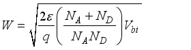 (2)
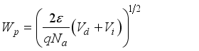
(2)  (3)
(3) 
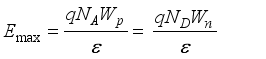
 (4)
(4)  (5)
(5)  —barrier height, Se and Sh—surface recombination velocity electron and hole, NC and NV —effective density of states, NAG —acceptor-like defect density, NDG —donor-like defect density, EA and ED —peak energy in,
  and,
and,  —capture cross section electrons and holes,
  —thermal velocity, WG —characteristic energy.
 Parameters | CIGS | CdS | ZnO |
|---|---|---|---|
W(nm) | 1000 | 30 | 100 |
Eg(eV) | 1,2 | 2,4 | 3,3 |
ᵡe(eV) | 4,5 | 4,45 | 4,45 |
ɛ/ɛ0 | 13,6 | 10 | 9 |
NC(cm-3) | 2,2x10¹⁸ | 2,2x10¹⁸ | 2,2x10¹⁸ |
NV(cm-3) | 1,8x10¹⁹ | 1,8x10¹⁹ | 1,8x10¹⁹ |
ʋe(cm/s) | 5x10⁶ | 107 | 107 |
ʋh(cm/s) | 5x10⁶ | 107 | 107 |
µe(cm2/Vs) | 102 | 102 | 102 |
µh(cm2/Vs) | 25 | 25 | 25 |
NA [cm-3] | 1,5x10¹² | - | - |
ND [cm-3] | - | 2,5x10¹⁶ | 1018 |
σe [cm2] | 10-16 | 10-12 | 10-14 |
σe [cm2] | 10-16 | 10-12 | 10-15 |
Parameters | Right | Left | |
Фb [eV] | Фbn=0,0 | Фbp=0,15 | |
Se [cm/s] | 107 | 107 | |
Sh [cm/s] | 107 | 107 | |
Reflectivity | 0,05 | 0,8 |
 (6)
(6)  (7)
(7)  (8)
(8) AMPS−1D | Analysis for Microelectronic and Photonic Structures |
CdS | Cadmium Sulfide |
CdTe | Cadmium Telluride |
CIGS | Copper Indium Gallium Selenide |
Cu(In,Ga)Se2 | Copper Indium Gallium Diselenide |
FF | Fill Factor |
JSC | Short Circuit Current Density |
MO | Molybdenum |
MoSe2 | Molybdenum Diselenide |
PV | Photovoltaic |
SCAPS-1D | One-dimensional Solar Cell Capacities Simulation |
SCR | Space Charge Region |
Vbi | Internal Potential |
VOC | Open Circuit Voltage |
WSCR | Space Charge Region Width |
ZnO | Zinc Oxide |
| [1] | Dupuis, J. 2009. Elaboration and characterization of SiOxNy: H and SiNx: H layers produced by the PECVD method: application to the back side of silicon photovoltaic cells. Ph. D. thesis, Institute of Nanotechnologies of Lyon (INSA Lyon). |
| [2] | Yan, X. 2014. Fabrication and characterization of CuInGaSe2 films by sputtering. Study of defects by deep-trapping spectroscopy by charge. Ph. D. thesis, University of Nantes. |
| [3] | Oubda, D., Kebre, M., Ouedraogo, S., Diasso, A., Zougmore, F., Koalga, Z., Ouattara, F. (2022) High Performance for Cu(In, Ga)Se2 Quaternary System-Based Solar Cells with Alternative Buffer Layers. Advances in Materials Physics and Chemistry, 12, 207-209. |
| [4] | Ouedraogo, S., Kebre, M. B., Ngoupo, A. T., Oubda, D., Zougmore, F., Ndjaka, J.-M. (2020) Required CIGS and CIGS/Mo Interface Properties for High-Efficiency Cu(In, Ga)Se2 Based Solar Cells. Advances in Materials Physics and Chemistry, 10, 151-166. |
| [5] | Zongo, A., Oubda, D., Ouedraogo, S., Kebre, M. B., Diasso, A., Sankara, I., Traore, B., Zougmore, F., Koalga, Z., Ouattara, F. (2021) Optimization of Mo/Cu(In,Ga)Se2/CdS/ZnO Hetero-Junction Solar Cell Performance by Numerical Simulation with SCAPS-1D. Journal of Materials Science and Engineering B, 11, 156-167. |
| [6] | Dullweber, T., Hanna, G., Shams-Kolahi., G., Schwartzlander, A., Contreras, M. A., Noufi, R., Schock, H. W. 2000. Study of the effect of gallium grading in Cu(In,Ga)Se2. Thin Solid Films, 361-362, 478–481. |
| [7] | Daouda, O., Marcel, B. K., Francois, Z., Donatien, N., Frederic, O. (2015) Numerical Simulation of Cu(In,Ga)Se2 Solar Cells Performances. Journal of Energy and Power Engineering, 9, 1047-105. |
| [8] | Oubda, D. (2018) Characterization of a Thin-Film Solar Cell Based on of CIGS Depending on the Nature of the Buffer Layer. University of Ouagadougou, Ouagadougou. |
| [9] | Oubda, D., Kebre M. B., Ouedraogo, S., Zougmore, F., Ouattara, F., Koalga, Z. (2018) Numerical Characterization of Cu(In, Ga)Se2 Solar Cells Using Capacitance-Voltage and Capacitance-Frequency Characteristics. International Journal of Progressive Sciences and Technologies, 6, 262-267. |
| [10] | Souici, F. 2009, Modeling of a thin layer solar cell based on Copper Indium Selenium (CuInSe2), magister. Kasdi Merbah Ouargla University. |
| [11] | Pettersson, J. 2012. Modelling band gap gradiens and Cd-free buffer layers in Cu(In,Ga)Se2 solar cells. Ph. D. thesis, Uppsalat University. |
| [12] | Kessler, F., Dominik, R. 2004. Technological aspects of flexible CIGS solar cells and modules. Solar Energy, 77 (2004), 685695. |
| [13] | Benaïcha, M. 2010. Fabrication of ternary thin films by electrochemical means. Physic-chemical and electrical characterization. Ph. D. thesis, Ferhat Abbas University of Sétif. |
| [14] | Painchaud, T. 2010. Growth mechanisms of co-evaporated Cu(In,Ga)Se2 thin films: towards rapid and low-temperature syntheses. Ph. D. thesis, University of Nantes. |
| [15] | Buffiere, M., Harel, S., Arzel, L., Deudon, C., Barreau, N., Kessler, J. 2011. Fast chemical bath deposition of Zn(O,S) thin films for Cu(In,Ga)Se2 solar cells. Thin Solid Films, 519, 575–7578. |
| [16] | Abou-Ras, D., Kostorz, G., Bremaud, D., Kelin, M., Kurdesau, F. V., Tiwari, A. N., Debeli, M. 2005. Formation and characterisation of MoSe2 for Cu(In,Ga)Se2 based solar cells. Thin Solid Films 480481 (2005) 433 438, 480481 (2005), 433 438. |
| [17] | Bollero, A., Kaupmees, L., Raadik, T., Grossberg, M., Fernández, S. 2011. Thermal stability of sputtered Mo/polyimide films and formation of MoSe2 and MoS2 layers for application in flexible Cu(In,Ga)(Se,S)2 based solar cells. Thin Solid Films, 2011, 6. |
| [18] | Wei-Ting, L., Shih-Hao, C., Shao-Ze, T., Jhih-Jian, H., Sheng-Hui, C., Ruei-Fu, S., Chien-Wei, T., Tomi, T., L., Sung-Cheng, H., Wan-Xuan, P., Yung-Tien, L. 2014. Manipulation of MoSe2 Films on CuIn(Ga)Se2 Solar Cells during Rapid Thermal Process. Hindawi Publishing Corporation International Journal of Photoenergy, 2014, 5. |
| [19] | Duchatelet, A. 2012. Synthesis of thin layers of Cu(In,Ga)Se2 for solar cells by electrodeposition of mixed copper-indium-gallium oxides. Ph. D. thesis, Lille1 University. |
| [20] | Ribeaucourt, L. 2011. Electrodeposition and selenization of Cu-In-Ga alloys for the synthesis of Cu(In,Ga)Se2 thin films for solar cells. Ph. D. thesis, Université Pierre et Marie Curie. |
| [21] | Gloeckler, M. 2005. Device physics of Cu(In,Ga)Se2 thin-film solar cells. Ph. D. thesis, Colorado State University. |
| [22] | Ouedraogo, S. 2016. Numerical modeling of a CIGS-based thin-film solar cell. Ph. D. thesis, University of Ouaga I Professor J. K. Zerbo. |
| [23] | Niemegeers, A., Burgelman, M., Herberholz, R., Rau, U., Hariskos, D., Schock, H.-W. 1998. Model for electronic transport in Cu(In,Ga)Se2 Solar Cells. Applied Physics Letters, 6, 407–421. |
| [24] | Khelifi, S., Belghachi, A. 2004. The Role of the Window Layer in the Performance of a GaAs Solar Cell. Rev. Energ. Ren., Vol. 7 (2004), 13–21. |
| [25] | Burgelman, M., Nollet, P., Degrave, S. 2000. Modelling polycrystalline semiconductor solar cells. Thin Solid Film, 361_362(2000); 527 -532: |
| [26] | Yiming, L., Yun, S., Angus, R. 2011. A new simulation software of solar cells-wxAMPS. Solar Energy Materials and Solar Cells, (2011), |
| [27] | Oubda, D., Diasso, A., Ouedraogo, B., Kabre, S., Kebre, M. B., Ouedraogo, S., Traore, B., Zongo, A., Sankara, I., Sawadogo, P., Barry, A., Sawadogo, B. and Zougmore, F. (2025) Numerical Simulation of the Dominate Recombination Mechanism in the Chalcopyrite Cu(In,Ga)Se2 Thin Film Solar Cell. Open Journal of Applied Sciences, 15, 3663-3672. |
| [28] | Oubda, D., Kabre S., Diasso A., Ouedraogo, B., Kebre M. B., Ouedraogo S., Traore B., Sankara I., Zongo, A., Barry A., Sawadogo B., Sawadogo P., Zougmore F. (2026) Simulation of the Effects of the Thickness and the Bandgap of the Absorber on the Performance of the Quaternary Thin Film Solar Cell Based on Cu(In,Ga)Se2 Doctoral School of Sciences and Technologies, Joseph KI-ZERBO University, Ouagadougou, Burkina Faso. American Journal of Energy Engineering 2026, Vol. 14, No. 1, pp. 1–8 |
| [29] | Ouedraogo, S., Kebre, M. B., Ngoupo, A. T., Oubda, D., Zougmore, F. (2020) Comprehensive Analysis of CuIn1−xGaxSe2 Based Solar Cells with Zn1−yMgyO Buffer Layer. Materials Sciences and Applications, 11, 880-892. |
| [30] | Ouedraogo S., Traore B., Kebre B. M., Oubda D., Zongo A., Sankara I., Zougmore F. (2020). Performance Enhancement Strategy of Ultra-Thin CIGS Solar Cells. American Journal of Applied Sciences, 2020, Volume 17, pp. 246 255. |
| [31] | Shou-Yi K., Ming-Yang H., Dan-Hua H., Hao-Chung K., Chyong-Hua C., Fang-I L. (2014). Device Modeling of the Performance of Cu(In,Ga)Se2 Solar Cells with V-Shaped Bandgap Profiles. |
| [32] | Pflieger J.-P., 2002. pn junction and diode. Marie and Louis Pasteur University. |
| [33] | Noël Servagent, 2004. Abrupt junction at thermodynamic equilibrium. Mens University, |
| [34] | Abdelkrim Naas, 2020. the pn junction. Frere Mentouri University, |
| [35] | E. Gorji, U. Reggiani, L. Sandrolini. "A simple model for the photocurrent density of a graded band gap CIGS thin film solar cell", Solar Energy, vol. 86, no. 3, p. 920-925, March 2012. |
APA Style
Oubda, D., Bayala, A., Koumbem, W. N. D., Coulibaly, Y., Zougmore, F. (2026). Numerical Simulation of the Performance of the Cu(In,Ga)Se2-based Solar Photovoltaic Cell as a Function of the Space Charge Region Width. American Journal of Modern Physics, 15(5), 140-147. https://doi.org/10.11648/j.ajmp.20261505.11
ACS Style
Oubda, D.; Bayala, A.; Koumbem, W. N. D.; Coulibaly, Y.; Zougmore, F. Numerical Simulation of the Performance of the Cu(In,Ga)Se2-based Solar Photovoltaic Cell as a Function of the Space Charge Region Width. Am. J. Mod. Phys. 2026, 15(5), 140-147. doi: 10.11648/j.ajmp.20261505.11
@article{10.11648/j.ajmp.20261505.11,
  author = {Daouda Oubda and Alfred Bayala and Winde Nongue Daniel Koumbem and Yacouba Coulibaly and Francois Zougmore},
  title = {Numerical Simulation of the Performance of the Cu(In,Ga)Se2-based Solar Photovoltaic Cell as a Function of the Space Charge Region Width},
  journal = {American Journal of Modern Physics},
  volume = {15},
  number = {5},
  pages = {140-147},
  doi = {10.11648/j.ajmp.20261505.11},
  url = {https://doi.org/10.11648/j.ajmp.20261505.11},
  eprint = {https://article.sciencepublishinggroup.com/pdf/10.11648.j.ajmp.20261505.11},
  abstract = {In a global context marked by constantly increasing energy demand, dwindling fossil fuel resources, and growing environmental concerns, the search for alternative, clean, and sustainable energy sources has become essential. Several questions remain regarding the production of abundant, low-cost energy without environmental impact. Therefore, optimizing the performance of thin-film photovoltaic (PV) solar cells has been the subject of numerous studies. Our study falls within this perspective and analyzes the role of the space charge region (SCR) in the performance optimization process. The aim of our study is to obtain improved electrical parameters. To achieve this objective, we opted for numerical simulation with One-dimensional Solar Cell Capacities Simulation software (SCAPS-1D) of the Mo/CIGS/CdS/ZnO structure. The results obtained show a significant decrease in the open circuit voltage (VOC) and the fill factor (FF) as the SCR width increases. The short-circuit current density (JSC) values increase with increasing SCR width and reach their maximum at a SCR value of 600 nm. As for the conversion efficiency, the values decrease for 100 nm≤ WSCR≤200 nm then remain almost constant for 200 nmSCRSCR≤700 nm). Future research will consider the effects of donor and acceptor density in the performance optimization process.},
 year = {2026}
}
TY  - JOUR
T1  - Numerical Simulation of the Performance of the Cu(In,Ga)Se2-based Solar Photovoltaic Cell as a Function of the Space Charge Region Width
AU  - Daouda Oubda
AU  - Alfred Bayala
AU  - Winde Nongue Daniel Koumbem
AU  - Yacouba Coulibaly
AU  - Francois Zougmore
Y1  - 2026/09/20
PY  - 2026
N1  - https://doi.org/10.11648/j.ajmp.20261505.11
DO  - 10.11648/j.ajmp.20261505.11
T2  - American Journal of Modern Physics
JF  - American Journal of Modern Physics
JO  - American Journal of Modern Physics
SP  - 140
EP  - 147
PB  - Science Publishing Group
SN  - 2326-8891
UR  - https://doi.org/10.11648/j.ajmp.20261505.11
AB  - In a global context marked by constantly increasing energy demand, dwindling fossil fuel resources, and growing environmental concerns, the search for alternative, clean, and sustainable energy sources has become essential. Several questions remain regarding the production of abundant, low-cost energy without environmental impact. Therefore, optimizing the performance of thin-film photovoltaic (PV) solar cells has been the subject of numerous studies. Our study falls within this perspective and analyzes the role of the space charge region (SCR) in the performance optimization process. The aim of our study is to obtain improved electrical parameters. To achieve this objective, we opted for numerical simulation with One-dimensional Solar Cell Capacities Simulation software (SCAPS-1D) of the Mo/CIGS/CdS/ZnO structure. The results obtained show a significant decrease in the open circuit voltage (VOC) and the fill factor (FF) as the SCR width increases. The short-circuit current density (JSC) values increase with increasing SCR width and reach their maximum at a SCR value of 600 nm. As for the conversion efficiency, the values decrease for 100 nm≤ WSCR≤200 nm then remain almost constant for 200 nmSCRSCR≤700 nm). Future research will consider the effects of donor and acceptor density in the performance optimization process.
VL  - 15
IS  - 5
ER  -
Materials and Environment Laboratory, Joseph Ki-Zerbo University, Ouagadougou, Burkina Faso
Thermal and Renewable Energy Laboratory, Joseph Ki-Zerbo University, Ouagadougou, Burkina Faso
Thermal and Renewable Energy Laboratory, Joseph Ki-Zerbo University, Ouagadougou, Burkina Faso
Laboratory of Materials, Heliophysics and Environment, Nazi Boni University, Bobo-Dioulasso, Burkina Faso
Materials and Environment Laboratory, Joseph Ki-Zerbo University, Ouagadougou, Burkina Faso
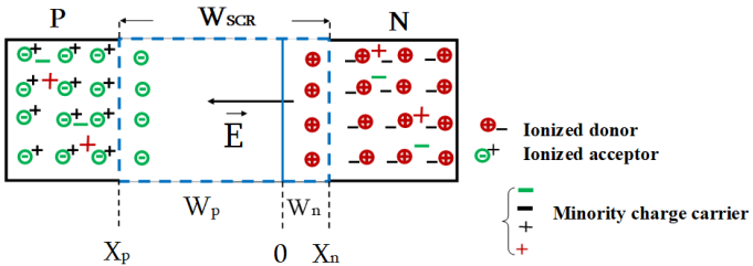
Figure 1. Model of the space charge region of a p-n junction and the explanation of the constituants elements.
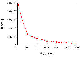
Figure 2. Evolution of the internal electric field as a function of the SCR width.
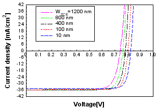
Figure 3. J-V curves as a function of the width of the SCR.
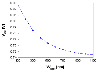
Figure 4. VOC as a function of SCR width.
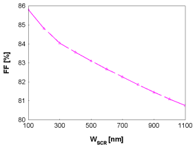
Figure 5. FF as a function of SCR width.
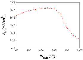
Figure 6. JSC as a function of SCR width.
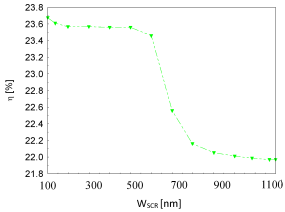
Figure 7. Conversion efficiency as a function of SCR width.
Table 1. Base parameters of CIGS cell properties. —barrier height, Se and Sh—surface recombination velocity electron and hole, NC and NV —effective density of states, NAG —acceptor-like defect density, NDG —donor-like defect density, EA and ED —peak energy in, and, —capture cross section electrons and holes, —thermal velocity, WG —characteristic energy. [3, 4, 5, 7, 22, 28-31].

Information



 Share This Article
 Twitter
 Linked In
 Facebook
 Copy
Copy Download